Over the course of the last year and a half, I ve been doing some self-directed
learning on how radios work. I ve gone from a very basic understanding of
wireless communications (there s usually some sort of antenna, I guess?) all
the way through the process of learning about and implementing a set of
libraries to modulate and demodulate data using my now formidable stash of SDRs.
I ve been implementing all of the RF processing code from first principals and
purely based on other primitives I ve written myself to prove to myself that I
understand each concept before moving on.
I figured that there was a fun capstone to be done here - the blind reverse
engineering and implementation of the protocol my cheep Amazon power switch
uses to turn on and off my Christmas Tree. All the work described in this post
was done over the course of a few hours thanks to help during the demodulation
from
Tom Bereknyei and
hlieberman.
Going in blind
When I first got my switch, I checked it for any FCC markings in order to look
up the FCC filings to determine the operational frequency of the device, and
maybe some other information such as declared modulation or maybe even part
numbers and/or diagrams. However, beyond a few regulatory stickers, there were
no FCC ids or other distinguishing IDs on the device. Worse yet, it appeared to
be a whitelabeled version of another product, so searching Google for the
product name was very unhelpful.
Since operation of this device is unlicensed, I figured I d start looking in
the ISM band. The most common band used that I ve seen is the band starting
at 433.05MHz up to 434.79MHz. I fired up my trusty waterfall tuned to a
center frequency of 433.92MHz (since it s right in the middle of the band, and
it let me see far enough up and down the band to spot the remote) and pressed
a few buttons. Imagine my surprise when I realize the operational frequency of
this device is 433.920MHz, exactly dead center. Weird, but lucky!
 After taking a capture, I started to look at understanding what the modulation
type of the signal was, and how I may go about demodulating it.
Using inspectrum, I was able to clearly
see the signal in the capture, and it immediately stuck out to my eye to be
encoded using OOK / ASK.
After taking a capture, I started to look at understanding what the modulation
type of the signal was, and how I may go about demodulating it.
Using inspectrum, I was able to clearly
see the signal in the capture, and it immediately stuck out to my eye to be
encoded using OOK / ASK.
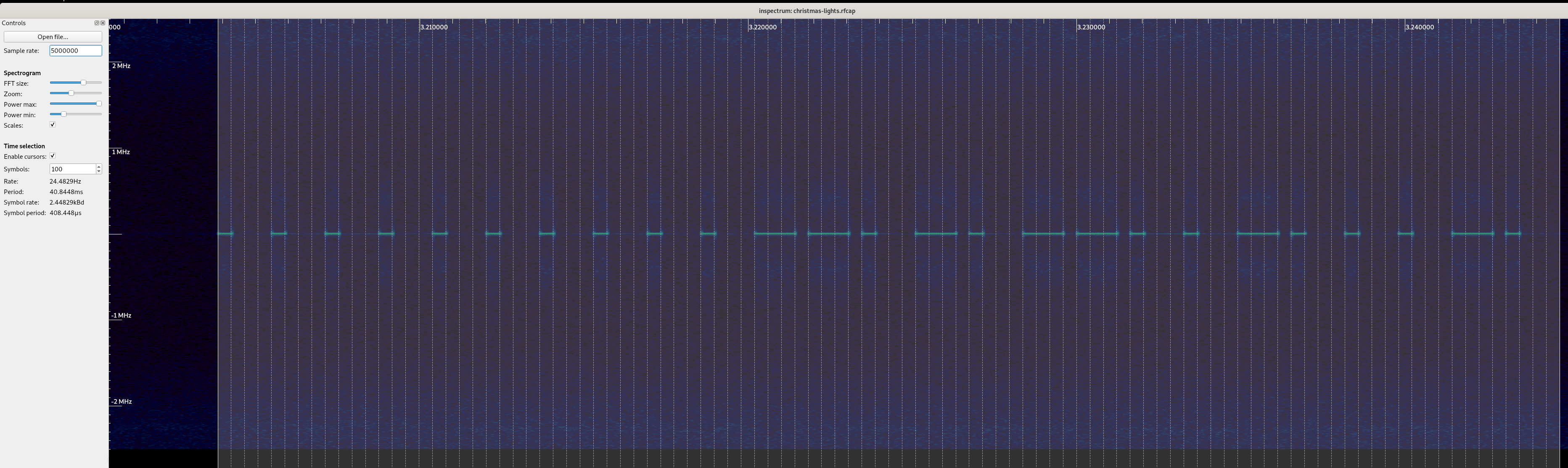
 Next, I started to measure the smallest pulse, and see if I could infer the
symbols per second, and try to decode it by hand. These types of signals are
generally pretty easy to decode by eye.
Next, I started to measure the smallest pulse, and see if I could infer the
symbols per second, and try to decode it by hand. These types of signals are
generally pretty easy to decode by eye.
 This wound up giving me symbol rate of 2.2 Ksym/s, which is a lot faster than I
expected. While I was working by hand, Tom
demodulated a few messages in Python, and noticed that if you grouped the bits
into groups of 4, you either had a
This wound up giving me symbol rate of 2.2 Ksym/s, which is a lot faster than I
expected. While I was working by hand, Tom
demodulated a few messages in Python, and noticed that if you grouped the bits
into groups of 4, you either had a 1000 or a 1110 which caused me to
realize this was encoded using something I saw documented elsewhere, where the
0 is a short pulse, and a 1 is a long pulse, not unlike morse code, but
where each symbol takes up a fixed length of time (monospace morse code?).
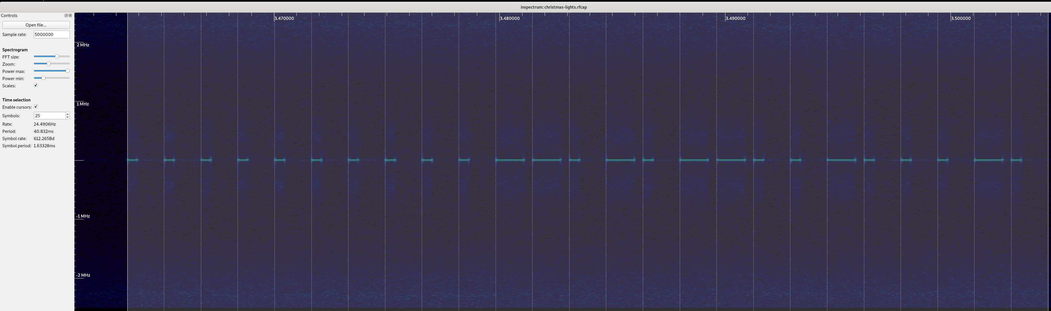
Working on that assumption, I changed my inspectrum symbol width, and
demodulated a few more by hand. This wound up demodulating nicely (and the
preamble / clock sync could be represented as repeating 0s, which is handy!)
and gave us a symbol rate of 612(ish) symbols per second a lot closer to
what I was expecting.
 If we take the code for on in the inspectrum capture above and demodulate
it by hand, we get
If we take the code for on in the inspectrum capture above and demodulate
it by hand, we get 0000000000110101100100010 (treat a short pulse as a 0, and
a long pulse as a 1). If you re interested in following along at home, click on
the inspectrum image, and write down the bits you see, and compare it to what
I have!
Right, so it looks like from what we can tell so far that the packet looks
something like this:
Next, I took a capture of all the button presses and demodulated them by hand,
and put them into a table to try and understand the format of the messages:
| Button |
Demod'd Bits |
| On |
0000000000110101100100010 |
| Off |
00000000001101011001010000 |
| Dim Up |
0000000000110101100110100 |
| Dim Down |
0000000000110101100100100 |
| Timer 1h |
0000000000110101100110010 |
| Timer 2h |
0000000000110101100100110 |
| Timer 4h |
0000000000110101100100000 |
| Dim 100% |
0000000000110101000101010 |
| Dim 75% |
00000000001101010001001100 |
| Dim 50% |
00000000001101010001001000 |
| Dim 25% |
0000000000110101000100000 |
Great! So, this is enough to attempt to control the tree with, I think so I
wrote a simple modulator. My approach was to use the fact that I can break down
a single symbol into 4 sub-symbol components which is to say, go back to
representing a
1 as
1110, and a
0 as
1000. This let me allocate IQ
space for the symbol, break the bit into 4 symbols, and if that symbol is 1,
write out values from a carrier wave (
cos in the
real values, and
sin in
the
imaginary values) to the buffer. Now that I can go from bits to IQ data,
I can transmit that IQ data using my PlutoSDR or HackRF and try and control my
tree. I gave it a try, and the tree blinked off!
Success!
But wait that s not enough for me I know I can t just demodulate bits and
try and replay the bits forever there s stuff like addresses and keys and
stuff, and I want to get a second one of these working. Let s take a look at
the bits to see if we spot anything fun & interesting.
At first glance, a few things jumped out at me as being weird? First is
that the preamble is 10 bits long (fine, let s move along - maybe it
just needs 8 in a row and there s two to ensure clocks sync?). Next is that
the messages are not all the same length. I double (and triple!) checked
the messages, and it s true, the messages are not all the same length. Adding
an extra bit at the end didn t break anything, but I wonder if that s just due
to the implementation rather than the protocol.
But, good news, it looks like we have a stable prefix to the messages from the
remote must be my device s address! The stable 6 bits that jump out right
away are
110101. Something seems weird, though, 6 bits is a bit awkward, even
for a bit limited embedded device. Why 6? But hey, wait, we had 10 bits in the
preamble, what if we have an 8 bit address meaning my device is
00110101,
and the preamble is 8
0 symbols! Those are numbers that someone working on
an 8 bit aligned platform would pick! To test this, I added a
0 to the
preamble to see if the message starts at the first
1, or if it requires all
the bits to be fully decoded, and lo and behold, the tree did not turn on or
off. This would seem to me to confirm that the 0s are part of the address,
and I can assume we have two 8 bit aligned bytes in the prefix of the message.
preamble / sync
address
stuff
Now, when we go through the 9-10 bits of stuff , we see all sorts of weird
bits floating all over the place. The first 4 bits look like it s either
1001 or
0001, but other than that, there s a lot of chaos. This is where
things get really squishy. I needed more information to try and figure this out,
but no matter how many times I sent a command it was always the same bits (so,
no counters), and things feel very opaque still.
The only way I was going to make any progress is to get another switch and see
how the messages from the remote change. Off to Amazon I went, and ordered
another switch from the same page, and eagerly waited its arrival.
Switch #2
The second switch showed up, and I hurriedly unboxed the kit, put batteries
into the remote, and fired up my SDR to take a capture. After I captured the
first button ( Off ), my heart sunk as I saw my lights connected to
Switch #1 flicker off. Apparently the new switch and the old switch have the
same exact address. To be sure, I demodulated the messages as before, and
came out with the exact same bit pattern. This is a setback and letdown I
was hoping to independently control my switches, but it also means I got no
additional information about the address or button format.
The upside to all of this, though, is that because the switches are controlled
by either remote, I only needed one remote, so why not pull it apart and see if
I can figure out what components it s using to transmit, and find any
datasheets I can. The PCB was super simple, and I wound up finding a WL116SC
IC on the PCB.
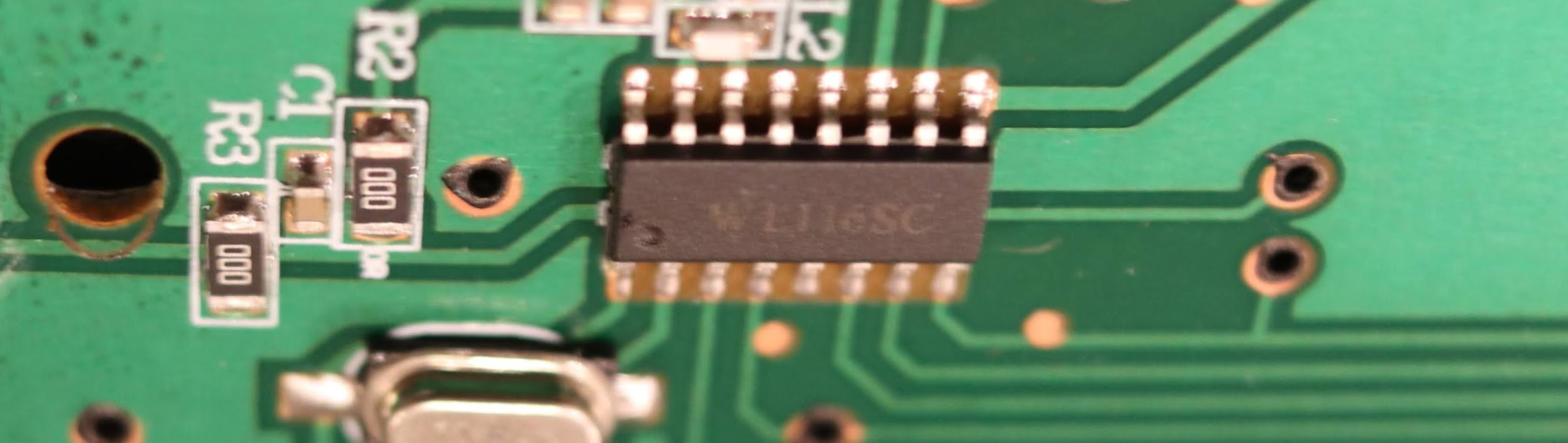 After some googling, I found a single lone
datasheet,
entirely in Chinese. Thankfully, Google Translate seems to have worked well
enough on technical words, and I was able to put together at least a little bit
of understanding based on the documentation that was made available. I took a
few screenshots below - I put the google translated text above the hanzi. From
that sheet, we can see we got the basics of the 1 and 0 symbol encoding
right (I was halfway expecting the bits to be flipped), and a huge find by way
of a description of the bits in the message!
After some googling, I found a single lone
datasheet,
entirely in Chinese. Thankfully, Google Translate seems to have worked well
enough on technical words, and I was able to put together at least a little bit
of understanding based on the documentation that was made available. I took a
few screenshots below - I put the google translated text above the hanzi. From
that sheet, we can see we got the basics of the 1 and 0 symbol encoding
right (I was halfway expecting the bits to be flipped), and a huge find by way
of a description of the bits in the message!
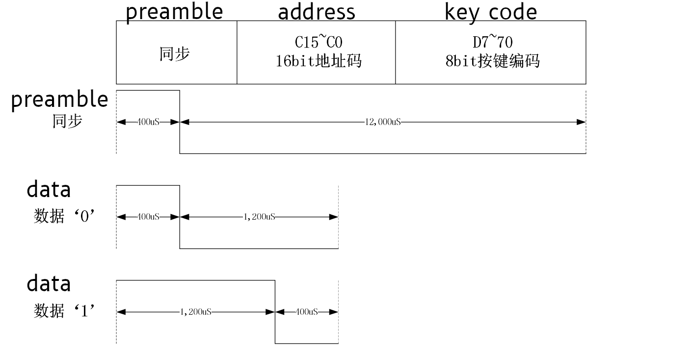 It s a bummer that we missed the clock sync / preamble pulse before the data
message, but that s OK somehow. It also turns out that 8 or 10 bit series of of
0"s wasn t clock sync at all - it was part of the address! Since it also turns
out that all devices made by this manufacturer have the hardcoded address of
It s a bummer that we missed the clock sync / preamble pulse before the data
message, but that s OK somehow. It also turns out that 8 or 10 bit series of of
0"s wasn t clock sync at all - it was part of the address! Since it also turns
out that all devices made by this manufacturer have the hardcoded address of
[]byte 0x00, 0x35 , that means that the vast majority of bits sent are always
going to be the same for any button press on any remote made by this vendor.
Seems like a waste of bits to me, but hey, what do I know.
Additionally, this also tells us the trailing zeros are not part of the data
encoding scheme, which is progress!
Now, working on the assumptions validated by the datasheet, here s the updated
list of scancodes we ve found:
| Button |
Scancode Bits |
Integer |
| On |
10010001 |
145 / 0x91 |
| Off |
10010100 |
148 / 0x94 |
| Dim Up |
10011010 |
154 / 0x9A |
| Dim Down |
10010010 |
146 / 0x92 |
| Timer 1h |
10011001 |
154 / 0x99 |
| Timer 2h |
10010011 |
147 / 0x93 |
| Timer 4h |
10010000 |
144 / 0x90 |
| Dim 100% |
00010101 |
21 / 0x15 |
| Dim 75% |
00010011 |
19 / 0x13 |
| Dim 50% |
00010010 |
18 / 0x12 |
| Dim 25% |
00010000 |
16 / 0x10 |
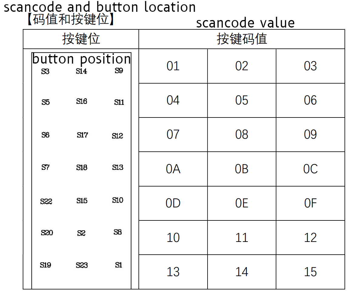
Interestingly, I think the Dim keys may have a confirmation that we have
a good demod the codes on the bottom are missing the most significant
bit, and when I look back at the scancode table in the datasheet, they make an
interesting pattern the bottom two rows, right and left side values match
up! If you take a look, Dim 100% is S1 , Dim 75% is S19 , Dim 50% is S8 ,
and Dim 25% is S20 . Cool!
Since none of the other codes line up, I am willing to bet the most significant
bit is a Combo indicator, and not part of the button (leaving 7 bits for the
keycode).
And even more interestingly, one of our scancodes ( Off , which is 0x94) shows up just
below this table, in the examples.
Over all, I think this tells us we have the right bits to look at for
determining the scan code! Great news there!
Back to the modulation!
So, armed with this knowledge, I was able to refactor my code to match the
timings and understanding outlined by the datasheet and ensure things still work.
The switch itself has a high degree of tolerance, so being wildly off frequency
or a wildly wrong symbol rate may actually still work. It s hard to know if
this is more or less correct, but matching documentation seems like a more stable
foundation if nothing else.
This code has been really reliable, and tends to work just as well as the
remote from what I ve been able to determine. I ve been using incredibly low
power to avoid any interference, and it s been very robust - a testament to the
engineering that went into the outlet hardware, even though it cost less than
of a lot of other switches! I have a lot of respect for the folks who built
this device - it s incredibly simple, reliable and my guess is this thing will
keep working even in some fairly harsh RF environments.
The only downside is the fact the manufacturer used the same address for all
their devices, rather than programming a unique address for each outlet and
remote when the underlying WL116SC chip supports it. I m sure this was done to
avoid complexity in assembly (e.g. pairing the remote and outlet, and having to
keep those two items together during assembly), but it s still a bummer. I took
apart the switch to see if I could dump an EEPROM and change the address in
ROM, but the entire thing was potted in waterproof epoxy, which is a very nice
feature if this was ever used outdoors. Not good news for tinkering, though!
Unsolved Mysteries
At this point, even though I understand the protocol enough to control the
device, it still feels like I hit a dead end in my understanding. I m not able
to figure out how exactly the scancodes are implemented, and break them down
into more specific parts. They are stable and based on the physical wiring of
the remote, so I think I m going to leave it a magic number. I have what I was
looking for, and these magic constants appear to be the right one to use, even
if I did understand how to create the codes itself.
This does leave us with a few bits we never resolved, which I ll memorialize
below just to be sure I don t forget about them.
Question #1: According to the datasheet there should be a preamble. Why do
I not see one leading the first message?
My hunch is that the trailing 0 at the end of the payload is actually just
the preamble for the next message (always rendering the first message
invalid?). This would let us claim there s an engineering reason why we are
ignoring the weird bit, and also explain away something from the documentation.
It s just weird that it wouldn t be present on the first message.
This theory is mostly confirmed by measuring the timing and comparing it to the
datasheet, but it s not exactly in line with the datasheet timings either
(specifically, it s off by 200 s, which is kinda a lot for a system using 400 s
timings). I think I could go either way on the last 0 being the preamble for
the next message. It could be that the first message is technically invalid, or
it could also be that this was not implemented or actively disabled by the
vendor for this specific application / device. It s really hard to know
without getting the source code for the WL116SC chip in this specific remote
or the source in the outlet itself.
Question #2: Why are some keycodes 8 bits and others 9 bits?
I still have no idea why there sometimes 8 bits (for instance, On ) and
other times there are 9 bits (for instance, Off ) in the 8 bit keycode
field.
I spent some time playing with the trailing zeros, when I try and send an
Off with the most significant 8 bits (without the least significant / last
9th bit, which is a 0 ), it does not turn the tree off. If I send an On with
9 bits (an additional 0 after the least significant bit), it does work,
but both On and Off work when I send 10, 11 or 12 bits padded with trailing
zeros. I suspect my outlet will ignore data after the switch is done reading
bits regardless of trailing zeros. The docs tell me there should only be 8 bits,
but it won t work unless I send 9 bits for some commands. There s something
fishy going on here, and the datasheet isn t exactly right either way.
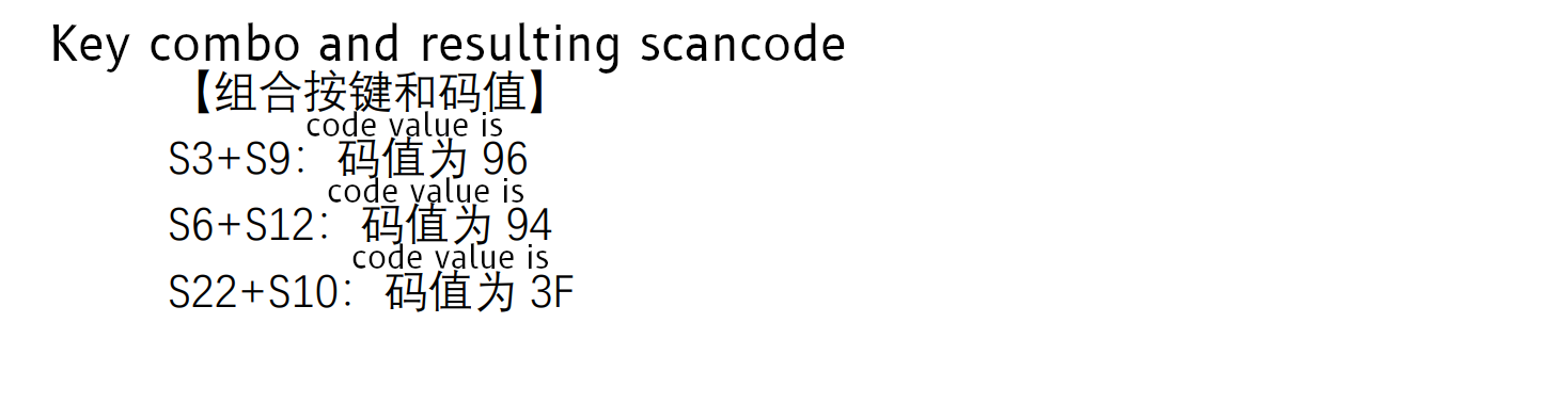
Question #3: How in the heck do those scancodes work?
This one drove me nuts. I ve spent countless hours on trying to figure this
out, including emailing the company that makes the WL116SC (they re really
nice!), and even though they were super kind and generous with documentation
and example source, I m still having a hard time lining up their documentation
and examples with what I see from my remote. I think the manufacturer of my
remote and switch has modified the protocol enough to where there s actually
something different going on here. Bummer.
I wound up in my place of last resort asking friends over Signal to try and
see if they could find a pattern, as well as making
multiple pleas to the twittersphere, to no avail (but thank you to
Ben Hilburn,
devnulling,
Andreas Bombe and Larme
for your repiles, help and advice!)
I still don t understand how they assemble the scan code for instance,
if you merely add, you won t know if a key press of 0x05 is 0x03 + 0x02
or if it s 0x01 + 0x04. On the other hand, treating it as two 4-bit
integers won t work for 0x10 to 0x15 (since they need 5 bits to
represent). It s also likely the most significant bit is a combo indicator,
which only leaves 7 bits for the actual keypress data. Stuffing 10 bits of data
into 7 bits is likely resulting in some really intricate bit work.
On a last ditch whim, I tried to XOR the math into working, but some initial
brute forcing to make the math work given the provided examples did not result
in anything. It could be a bitpacked field that I don t understand, but I don t
think I can make progress on that without inside knowledge and much more work.
Here s the table containing the numbers I was working off of:
| Keys |
Key Codes |
Scancode |
| S3 + S9 |
0x01 + 0x03 |
0x96 |
| S6 + S12 |
0x07 + 0x09 |
0x94 |
| S22 + S10 |
0x0D + 0x0F |
0x3F |
If anyone has thoughts on how these codes work, I d love to hear about it! Send
me an email or a tweet or something - I m a bit stumped.
There s some trick here that is being used to encode the combo key in a way
that is decodeable. If it s actually not decodeable (which is a real
possibility!), this may act as a unique button combo hash which allows the
receiver to not actually determine which keys are pressed, but have a unique
button that gets sent when a combo is used. I m not sure I know enough to
have a theory as to which it may be.
 About a month later than I probably should have posted it, here s a recap of my Free Software activities in 2021. For previous years see 2019 + 2020. Again, this year had fewer contributions than I d like thanks to continuing fatigue about the state of the world, and trying to work on separation between work and leisure while working from home. I ve made some effort to improve that balance but it s still a work in progress.